North American EMS Industry Down 2.4 Percent in June

IPC releases EMS Industry results for June 2024

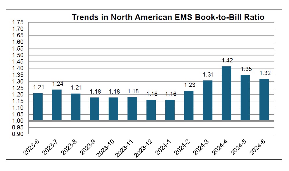
IPC announced today the June 2024 findings from its North American Electronics Manufacturing Services (EMS) Statistical Program. The book-to-bill ratio stands at 1.32.

Total North American EMS shipments in June 2024 were down 2.4 percent compared to the same month last year. Compared to the preceding month, June shipments decreased 3.3 percent.

EMS bookings in June decreased 3.5 percent year-over-year and decreased 2.8 percent from the previous month.

“EMS shipments were weak in June, but an even lower order flow kept the book-to-bill ratio stable, masking building weakness in the EMS sector,” said Shawn DuBravac, IPC’s chief economist.

July 2024 EMS book to bill ratio chart

Detailed Data Available

Companies that participate in IPC’s North American EMS Statistical Program have access to detailed findings on EMS sales growth by type of production and company size tier, order growth and backlogs by company size tier, vertical market growth, the EMS book-to-bill ratio, 3-month and 12-month sales outlooks, and other timely data.

Interpreting the Data

The book-to-bill ratios are calculated by dividing the value of orders booked over the past three months by the value of sales billed during the same period from companies in IPC’s survey sample. A ratio of more than 1.00 suggests that current demand is ahead of supply, which is a positive indicator for sales growth over the next three to twelve months. A ratio of less than 1.00 indicates the reverse.

Year-on-year and year-to-date growth rates provide the most meaningful view of industry growth. Month-to-month comparisons should be made with caution as they reflect seasonal effects and short-term volatility. Because bookings tend to be more volatile than shipments, changes in the book-to-bill ratios from month to month might not be significant unless a trend of more than three consecutive months is apparent. It is also important to consider changes in both bookings and shipments to understand what is driving changes in the book-to-bill ratio.

IPC’s monthly EMS industry statistics are based on data provided by a representative sample of assembly equipment manufacturers selling in the USA and Canada. IPC publishes the EMS book-to-bill ratio by the end of each month.

A Fully Additive Approach for High-Density Interconnect Printed Circuit Boards

Member Download (pdf)

High-density interconnect printed circuit boards (HDI PCBs) technology is evolving to enable further miniaturization and functionality of electronics like smartphones, tablet computers, and wearable devices. Therefore, miniaturization of copper lines and spaces (L/S) down to 5/5μm and possibly even lower is needed to add more layers and components without increasing the size, weight, or volume of the PCB. The development of fully additive fabrication techniques that are flexible, precise, uniform, cost-effective, and environmentally friendly is urgently needed for creating next-generation miniaturized HDI PCBs. This study reports a fully additive manufacturing method called sequential build-up-covalent bonded metallization (SBU-CBM) for the fabrication of miniaturized copper interconnects. Optical microscopy and scanning electron microscopy (SEM) imaging confirm the formation of robust copper interconnects with a feature size of L/S-5/5μm. Energy-dispersive x-ray spectroscopy (EDX) analysis demonstrates detailed information about selective copper metallization in the SBU-CBM method.

Author(s)
Roghayeh Imani, Sarthak Acharya, Jussi Putaala, Shailesh Chouhan, Juha Hagberg, Sami Myllymäki, Olli Nousiainen, Heli Jantunen, Jerker Delsing
Resource Type
Technical Paper
Event
IPC APEX EXPO 2023

Thermal Stress Reliability of Stacked Microvias Fabricated with a Liquid Metal Ink Semi-Additive Process

Member Download (pdf)

Latent reliability issues with stacked filled microvia designs for complex printed circuit boards fabricated using subtractive-etch processes have been well-documented in recent years. This issue is broadly defined as a weak interface between the plated copper and the blind via target pad. When thermally stressed, the generally weak interface will fracture, especially during forced-convection assembly reflow [1].

While many studies of microvia interfacial fracture focused on conventional electroless copper as the plated through hole (PTH) choice, no recent studies measured the reliability of stacked microvias with a semi-additive process (SAP) using a liquid metal ink technology as the catalytic layer.

To measure the reliability of the liquid metal ink process, a six-layer test vehicle was constructed: Layers 1 and 2 and layers 5 and 6 were fabricated with a liquid metal ink technology for additive processing. The conductive layers of the test vehicle were of 25-micron lines and 50-micron spaces.

Test vehicles were subject to 6× reflow simulation—according to protocols in IPC-TM-650 test method 2.6.27B, Thermal Stress, Reflow Simulation—followed by thermal shock reliability testing of 100 cycles with extremes of -65° to 150° C. IPC D-coupons were populated on the test vehicle with a microvia diameter of 100 microns, for an aspect ratio of 0.33:1. The test vehicle contained two sets of two-stack vias, plated copper filled.

For each thermal stress method, a 5% increase in resistance was considered a failure. However, none of the coupons in this test reached the 5% failure threshold. This paper will cover complete results of this study (and additional data from ongoing testing) to show that this technology holds promise for improvement of stacked microvia reliability.

Author(s)
Gus Karavakis, Mike Carano
Resource Type
Technical Paper
Event
IPC APEX EXPO 2023

Chemical and Microscopic Analyses of Laser Microvia Samples

Member Download (pdf)

Critical failures were found on laser-drilled microvias on printed wiring boards (PWBs). The copper-filled vias and their corresponding copper landing pads are on the order of 100 microns in diameter. The goal of this work was to examine the mating surfaces of microvias and pads from both good and failed parts for chemical contaminants that might be preventing metal-to-metal bonding between the microvias and their corresponding pads during electroplating of copper. This, in turn, could lead to detachment and electrical failures. Microvia (MV) samples (MV-1, MV-2, and MV-3) were investigated using Raman and x-ray photoelectron spectroscopy, and both optical and scanning electron microscopies. These analyses revealed cuprous oxide (Cu2O) crystals, 100-500 nm in size, on the interfaces of the vias and pads, especially at or near the rims. The pads and vias on sample MV-2 had the highest amounts of Cu2O contamination. X-ray CT scans showed that vias in MV-2 had cavities in the interior. In contrast, vias in MV-1 were completely filled. From the measurements it was concluded that the cause of detachment between the copper-filled via and its mating copper pad was the deposition of Cu2O crystals at the pad-via interface. A pathway to Cu2O deposition has been proposed whereby insufficient rinsing could leave behind a residual electroless copper (Cu) solution with a high pH along the rims of vias and pads. This high-pH liquid containing copper precursors can potentially lead to the electrolytic deposition of Cu2O at the start of the next step, namely, Cu electroplating.

Author(s)
Gouri Radhakrishnan, Paul M. Adams, Andrew J. Clough, Albert Ugarte, Eric B. Frasco, Neil A. Ives, Shawn P. Ashley
Resource Type
Technical Paper
Event
IPC APEX EXPO 2023

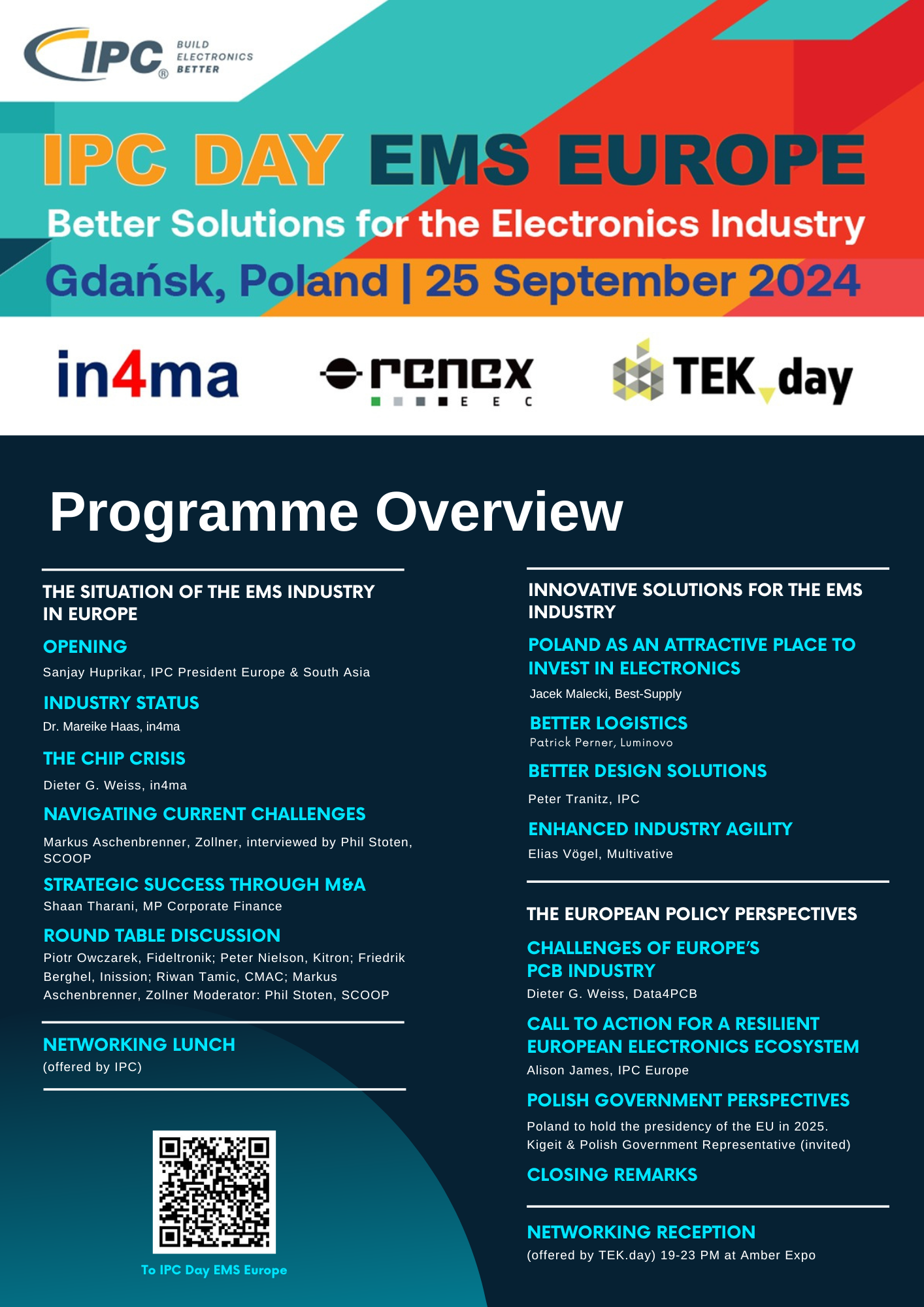
IPC Day EMS Europe Gdansk, Poland

Date
-

IPC Day EMS Europe: Better Solutions for the Electronics Industry

On Wednesday 25 September 2024, IPC EMS Day in Gdansk, Poland, will bring together leaders & experts from across the Electronics Manufacturing Services (EMS) industry to address the most pressing challenges, trends & innovations shaping the sector today. 

IPC Day EMS Europe will provide participants with deep insights into the European EMS landscape, explore solutions for navigating current obstacles & discuss policy perspectives that will shape the future of electronics manufacturing.

The event will provide a unique opportunity to learn about the latest advancements in electronics manufacturing, participate in industry discussions & network with a community of professionals dedicated to building electronics better.

Topics include:

  • State of the EMS industry in Europe, including implications of the chip crisis
  • Strategic success through M&A
  • Innovative solutions for the EMS industry: better logistics, better design solutions as well as an enhanced industry agility
  • Perspectives on European policy: challenges, call to action for a resilient European electronics ecosystem& Polish government perspectives, since Poland will be taking over the presidency of the EU in 2025. 


Please have a look at the programme: 

IPC Day EMS Europe 2024 programme

Where: AmberExpo, Żaglowa 11, 80-560, Gdansk, Poland

When: 25 September 2024, 09:00-17:00 h

Who should attend:

  • Manufacturing, quality and design engineers
  • Members of Academia
  • Senior & junior engineering students
  • Specialists or practitioners in manufacturing


North American PCB Industry Sales Up 1.0 Percent in June

IPC releases PCB industry results for June 2024

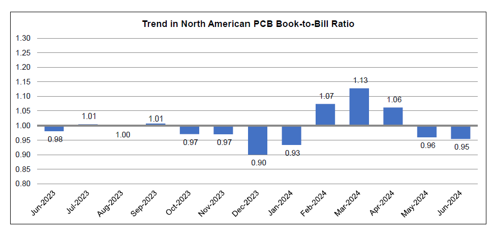
IPC announced today the June 2024 findings from its North American Printed Circuit Board (PCB) Statistical Program. The book-to-bill ratio stands at 0.95.

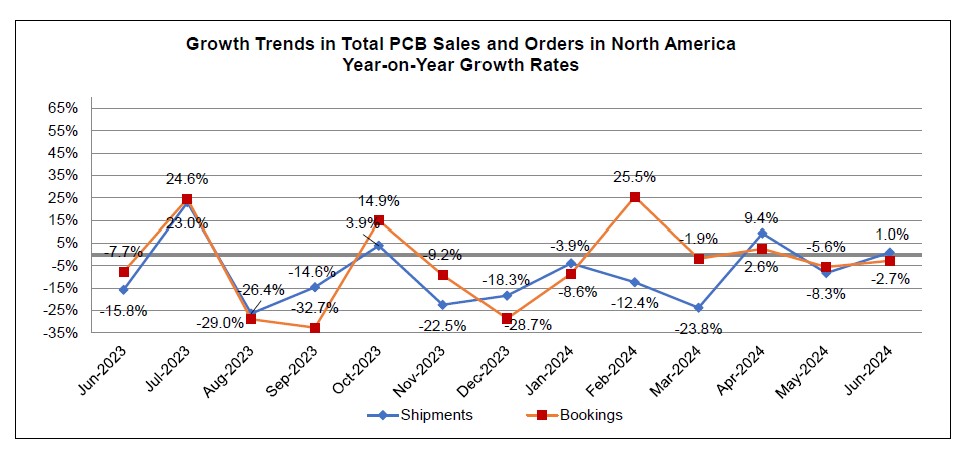
Total North American PCB shipments in June 2024 were up 1.0 percent compared to the same month last year. Compared to the preceding month, June shipments were up 9.1 percent.

PCB bookings in June were down 2.7 percent compared to the same month last year. June bookings were up 3.2 percent compared to the preceding month.

“The PCB sector recorded a strong month of shipments, outpacing orders and slightly pulling down the PCB book-to-bill ratio,” said Shawn DuBravac, IPC’s chief economist. “While production output remains healthy, there are potential challenges in maintaining the balance between supply and demand in the coming months.”

July 2024 PCB book to bill ratio chart 1
July 2024 PCB book to bill ratio chart 2

Detailed Data Available

Companies that participate in IPC’s North American PCB Statistical Program have access to detailed findings on rigid PCB and flexible circuit sales and orders, including separate rigid and flex book-to-bill ratios, growth trends by product types and company size tiers, demand for prototypes, sales growth to military and medical markets, and other timely data.

Interpreting the Data

The book-to-bill ratios are calculated by dividing the value of orders booked over the past three months by the value of sales billed during the same period from companies in IPC’s survey sample. A ratio of more than 1.00 suggests that current demand is ahead of supply, which is a positive indicator for sales growth over the next three to twelve months. A ratio of less than 1.00 indicates the reverse.

Year-on-year and year-to-date growth rates provide the most meaningful view of industry growth. Month-to-month comparisons should be made with caution as they reflect seasonal effects and short-term volatility. Because bookings tend to be more volatile than shipments, changes in the book-to-bill ratios from month to month might not be significant unless a trend of more than three consecutive months is apparent. It is also important to consider changes in both bookings and shipments to understand what is driving changes in the book-to-bill ratio.

IPC’s monthly PCB industry statistics are based on data provided by a representative sample of both rigid PCB and flexible circuit manufacturers selling in the USA and Canada. IPC publishes the PCB book-to-bill ratio by the end of each month.

IPC Education Foundation (IPCEF) Named Scholarship Provider for Opportunity Next Colorado

The IPC Education Foundation (IPCEF) promotes opportunities for students to access information and financial assistance for careers in the electronics manufacturing industry.  In addition to the existing IPC Scholarship and Award program, which has awarded more than $200,000 since 2019, the IPCEF was selected as one of the Opportunity Next Colorado Scholarship Program recipients.

The Opportunity Next Colorado Scholarship Program aims to increase enrollment in Colorado-based postsecondary education and training programs by prioritizing learners who pursue an in-demand or high-priority pathway. Scholarships are awarded to all eligible students who intend to enroll at a university or college to pursue an in-demand or high-priority postsecondary pathway or to students who intend to participate in a registered apprenticeship program. Each scholarship award provides a maximum of $1,500 per recipient. The student can use scholarship money for tuition, fees, and books.

“This opportunity aligns perfectly with our commitment and efforts to build a talent pipeline for the electronics manufacturing industry. What better way to support talented aspiring engineers in their next steps towards pursuing careers within the industry?” shared Charlene Gunter, senior director of IPCEF. “Meeting the students virtually via Zoom, seeing the excitement about the next chapter in their lives, and learning more about their career interests in becoming (electronics, aeronautical, mechanical) engineers cemented the positive impact this scholarship has for each one of them. We are grateful to Opportunity Next Scholarship Program for entrusting us with the award, and we are excited to play a small part in these students’ future careers.”

IPC, IPCEF’s parent organization, has successfully assisted OEMs, EMS, PCB manufacturers, cable and wire harness manufacturers, and electronics industry suppliers for 67 years. More than 3,200 companies worldwide depend on IPC programs and services to further their competitive advantage and financial success, including identifying skilled workers. 

IPCEF's relationship with local high schools, community colleges, and universities in Colorado has enabled IPCEF to support students beyond their existing programs. One of the schools that participated in a select program, the LPS Explorative Pathways for Innovative Careers "EPIC" Campus, officially opened in August 2023, produced 10 students benefiting from this opportunity.

EPIC’s programs allow students to experience hands-on learning using state-of-the-art technology and innovative processes. Educational pathways aligned to industry standards will focus on the following areas: aerospace, business and entrepreneurship, computer science, construction trades, future educators, health science, and natural resources.

Travis Amonson, Principal at EPIC Campus shared the following statement, “The EPIC Campus in Littleton, Colorado, was fortunate to receive grant funding at the end of the 2023-2024 school year from IPC through Opportunity Next. There were 10 recipients of scholarships. All 10 students plan to attend college and major in a degree related to the aerospace industry. At the EPIC Campus, students participated in the Aerospace Pathway, which offers classes related to Aerospace Engineering, Advanced Manufacturing, and Electronics. Students could take these classes, better understand the work, and make an educated decision about future plans. We are incredibly grateful for the partnership with IPC and the grant funding as it will certainly help students and their families as they pursue their degrees.”

IPC and IPCEF continue to look for opportunities to support the industry by identifying talent hubs for future employment. Victoria Hawkins, IPC director of workforce grants and proposals, stated, “We’ve been awarded $15,000 through this program and made a difference in 10 highly deserving student graduates from a Colorado high school, EPIC Campus. Our partnership with EPIC is unique, and this scholarship will support these students’ next steps in pursuing undergraduate degrees in an in-demand or high-priority postsecondary pathway, which includes engineering and technology and advanced manufacturing.”

Interested recent high school graduates who would like to learn more about this scholarship opportunity and in need of financial support whilst pursuing a degree at a local Colorado-based university can visit the following website and complete the interest form: https://www.ipcef.org/opportunity-next-colorado.

For more information on the grant opportunity, IPC, IPCEF and EPIC, visit the links below:

Grant information: https://oedit.colorado.gov/programs-and-funding/opportunity-next-colorado

IPCEF: http://ipcef.org/

IPC: https://www.ipc.org/

EPIC: https://littletonpublicschools.net/schools/epiccampus/welcome
Controlling Recrystallisation in Plated Layers Through the Use of Additives

Member Download (pdf)

This work compares the influence of a plating additive that has been applied to a commercially available electroless copper system and how its use impacts the morphology of the overall final plated structure. Through testing on insulating materials in addition to single and polycrystalline copper substrates, each electroless Cu solution is shown to be influential in suppressing grain growth in certain crystal orientations, which can lead to significant physical differences across the final plated interface. It is interesting to note that while the degree of epitaxy between the substrate Cu and the electroless Cu can be influenced dependent upon the additive utilized, this can occur independent of the impact between the electroless and electrolytic Cu. To wit, an epitaxial interface between the substrate and electroless Cu is not strictly indicative that an epitaxial structure will occur between the electroless and electrolytic Cu.

The plating additive under investigation is shown to support epitaxial or “bottom-up” recrystallisation for selective grain orientations originating within the substrate material and will typically facilitate grain growth in the (100) and (110) orientations while a solution without the additive supports the (110) and (111) orientations. Such performance is offered as occurring as a result of the characteristic electroless copper surface which consists predominantly of large, but low index {100} facets, in contrast to the smaller but higher order facets {221} that occur when the additive is not employed. When applied to polycrystalline substrates, either of the electroless copper processes considered within this investigation have been shown to facilitate a fully epitaxial structure, which arises from the situation that either of the “preferred” crystal orientations are available within the substrate.

Through careful selection of the additive packages used within an electroless Cu system, there can be significant control gained over how not only the electroless layer itself crystalizes, but also the response of the subsequent electroplated layer as well. Both of these are understood to have significant impact on the physical and mechanical properties of such an interface, which in turn can be influential in achieving the desired overall properties.

Through an increased understanding of how the additives used in a state-of-the-art electroless copper process function, and the impact that they subsequently have on the crystallography of the final deposit, it is anticipated that an improved overall joint integrity can be achieved. It is now considered that a fully epitaxial microstructure across the target pad – ELESS – ELYTC Cu interfaces is desirable as this offers a higher resistance to crack propagation and so enhances overall reliability. This is clearly beneficial in many plating applications, especially those containing microvias, where historically decreasing dimensions and aggressive operational demands in combination with an increased use of stacked BMV designs has led to undesirable interconnect failures around the target pad – electroless Cu – electroplated Cu interface.

Author(s)
T. Bernhard, R. Massey, K. Klaeden, S. Zarwell, E. Steinhaeuser, S. Kempa, F. Bruening
Resource Type
Technical Paper
Event
IPC APEX EXPO 2023

Reliability Impact of Frequent Power Cycles on Base Printed Wiring Boards High Density Packaging User Group (HDP)

Member Download (pdf)

The High Density Packaging (HDP) user group has completed a project to evaluate the impact on field reliability of more frequent thermal cycling over more narrow operating temperature ranges such as occur in today’s data center or cloud environments. In the past, printed wiring board field reliability testing assumed just one thermal cycle per day based upon systems begin completely shut off in the evening and circuit temperatures dropping to ambient temperature before being turned on again every morning. Whereas many systems today are rebooted and/or go into a lower power “sleep” mode ten or more times per day. In addition to the above new field application environments, laminate materials today have higher filler content and their mechanical characteristics are different from the less thermally robust phenolic and dicy-based laminate materials used prior to the widespread use of high temperature lead-free solder alloys in board assembly. Note that this project concerns the reliability of the bare printed wiring board and has no connection with any earlier “power cycling” projects which evaluated the reliability of various SMT or PTH solder joint alloys.

The goal of this project was to determine the relative impact on field reliability of more frequent thermal cycling over a more narrow temperature range with less frequent temperature cycling over a larger temperature range using at least two of the laminate materials available today. Interconnect Stress Testing (IST) is one of the recognized standards for measuring the expected reliability of bare printed wiring boards. Although there are other methods, the more practical IST method was selected for determining the impact of these new field conditions on printed wiring board reliability.

For both laminate material test lots, which had several physical differences, the results show that more frequent thermal cycling can significantly affect long term field reliability even with reduced temperature cycling ranges.

Author(s)
Karl Sauter, Joe Smetana
Resource Type
Technical Paper
Event
IPC APEX EXPO 2023

Root Cause Analysis and Risk Assessment of a Multilayer Ceramic Capacitor Flexural Crack Propagating Fault

Member Download (pdf)

Failure of a printed circuit board assembly (PCBA) can occur because of design, manufacturing, mechanical, or electrochemical issues. A propagating fault is a severe failure mechanism in which smoke, electrical arcing, and/or thermal degradation occurs. This paper details root cause failure analysis of a PCBA propagating fault resulting from flexure-induced capacitor cracking. This investigation also included optimization of design and qualification practices to reduce the risk of flexural crack induced failures.

Multilayer ceramic capacitors (MLCCs) are susceptible to flexural crack failure resulting from high strain inducing events, like bending or warpage. The PCBA in this study includes an array of MLCCs that initiated the propagating fault. The MLCCs are in a high strain region of the assembly, which created a short circuit when the flexural cracks propagated across opposing electrodes. The strain level on the MLCCs was exacerbated by adverse warpage conditions and proximity to rigid mounting constraints. Dynamic strains were a contributing factor due to a partially unsupported module directly adjacent to the capacitor array. The dynamic stain on the MLCCs, combined with residual strain, exceeded the strain threshold for the capacitor. Root cause was confirmed through physical analysis and finite element analysis (FEA).

Root cause failure analysis included an assessment to prevent reoccurrence of capacitor induced failures. PCBA and system design factors were evaluated to improve quality and reliability. Future design recommendations were provided, including implementing capacitor spacing guidelines, evaluating layout/component placement to reduce warpage, and employing FEA modeling to evaluate high strain regions.

Author(s)
Jennifer Bennett, Eric Campbell, Jim Bielick, Mehdi Hamid, Kevin O’Connell
Resource Type
Technical Paper
Event
IPC APEX EXPO 2023