IPC E-Textiles A-Team Wins Golden Gnome Award
Congratulations to Smarties, the IPC E-Textiles A-Team that developed the initial draft content for IPC-8981 and its IPC Test Methods, which won the Worker Bees of the Year Award. This award is given to A-Teams that have shown the most activity in IPC Works in development of their standard during the eligibility range for that year’s awards. IPC Works is the intranet collaboration site all IPC working groups use for their standards development efforts.
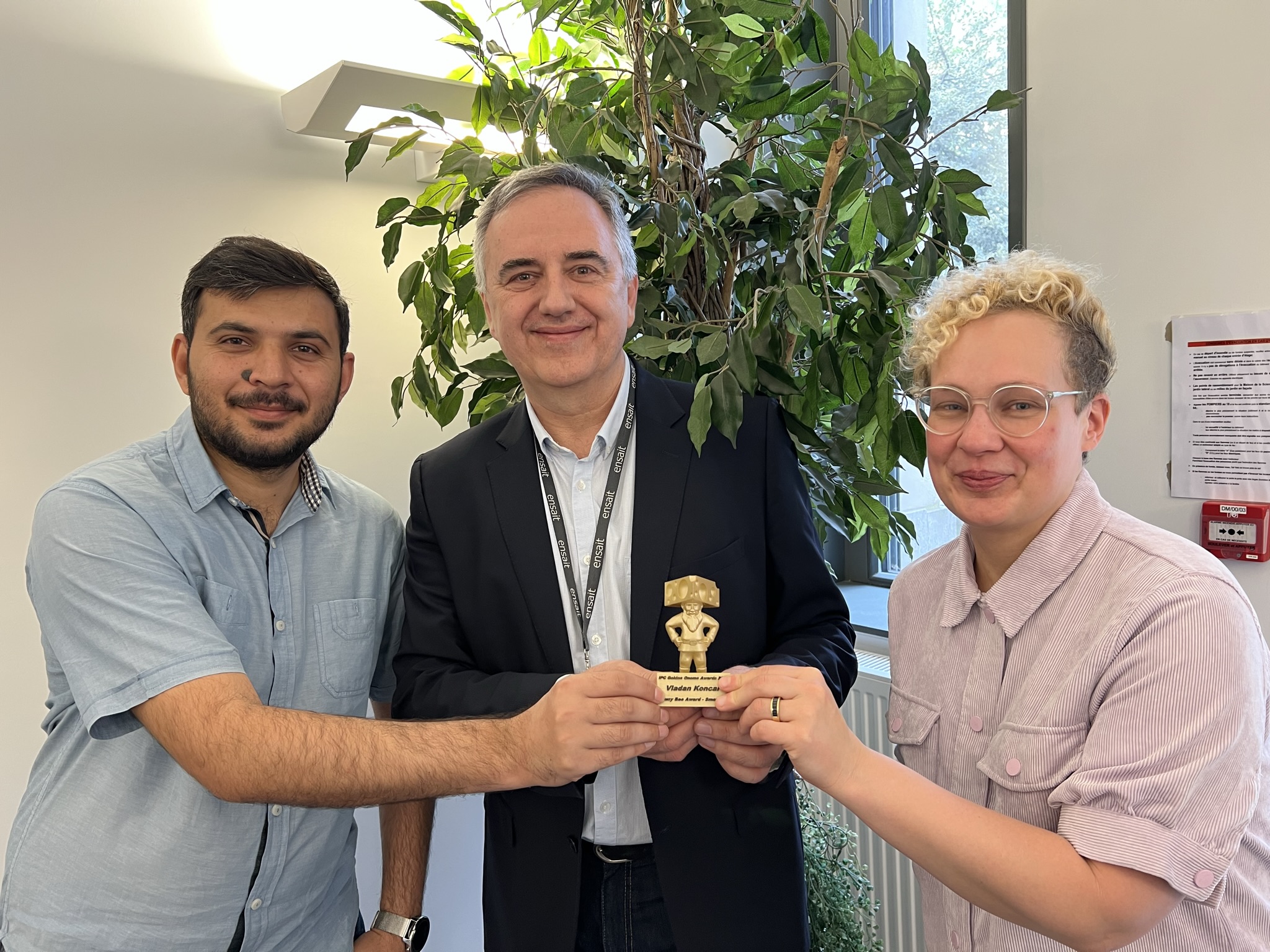
The award was announced during the 2nd Annual IPC Golden Gnome Awards during IPC SummerCom 2022 in Milwaukee, WI, USA. Smarties chair Vladan Koncar, ENSAIT GEMTEX Lab, University of Lille; vice-chair Sigrid Rotzler, Fraunhofer Institute for Reliability and Microintegration IZM and team member Shahood uz Zaman, National Textile University accepted the award on behalf of their A-Team.
Smarties Members Accept Their 2022 Golden Gnome for Worker Bees of the Year
(L-R, Shahood uz Zaman, National Textile University; Vladan Koncar, ENSAIT GEMTEX Lab, University of Lille; Sigrid Rotzler, Fraunhofer Institute for Reliability and Microintegration IZM)
The IPC Golden Gnome Awards recognize IPC A-Teams and their members for their participation in IPC standards development. These awards were inspired by the fictional TechNet gnomes, Clumpy and Kloumpios, who have become the mascots for IPC’s A-Teams. Awards are divided into two main categories – Clumpy and Kloumpios – with specific awards and recognitions under each category. Clumpy Awards are objective awards, based on voting and/or data. Kloumpios Awards are subjectively selected awards. Awardees are recognized during the Annual IPC Golden Gnomes Awards Ceremony held during IPC SummerCom. Each awardee is presented with a one-of-a-kind Golden Gnome statue, which has been created by an IPC staff liaison using a 3D printer.
Smarties Members
- Stefan Benedict, MAS Holdings PVT LTD
- Nuwan Chathuranga, MAS Holdings PVT LTD
- Ishan Chathuranga, University of Calgary/ Faculty of Kinesiology
- Joe Geiger, Bally Ribbon Mills
- Abiodun Komolafe, Abiodun O Komolafe
- Vladan Koncar, ENSAIT GEMTEX Lab, University of Lille
- Patricia Kowalski, Myant, Inc.
- Lim Ming, Jabil Circuit Sdn. Bhd.
- Oona Oksjarvi, Jabil
- Pratyush Rai, Nanowear Inc.
- Salwa Rasheed, Oculus Redmond Research Lab
- Sahar Rostami, Myant, Inc.
- Sigrid Rotzler, Fraunhofer Institute for Reliability and Microintegration IZM
- Paula Veske, Universiteit Gent
- Shahood uz Zaman, National Textile University