Evaluations onThe Mixing andReliability Testingof Tin-Bismuth Pastes withSnAgCu BGA Components andReliability Failure Analysis Comparing CT (Computed Tomography) Inspection andCross-Sectioning

Member Download (pdf)

Recently there has been an increase in the evaluation of low temperature lead-free soldering materials, such as tin-bismuth, in a process known as “hybrid assembly” in which higher temperature SnAgCu BGA/CSP components are assembled using low temperature tin-bismuth based pasts at typical tin-bismuth paste reflow soldering temperatures. One of the concerns in terms of assembly and reliability is the mixing of the high and low temperature alloys and its influence on reliability. A study was done to compare a series of tin-bismuthbased solder pastes (Sn58Bi, Sn57.6Bi0.4Ag, Alloy A, Alloy B, Alloy C, Alloy D)assembled with higher temperature SnAgCu BGA daisy-chained components and SnAgCu paste with SnAgCu BGA components in terms of thermal cycle reliability testing from -40°C to +125°C. Thereliability test vehicles (RTV) were thermally cycled from -40°C to +125°C until failure up to 3,000 thermal cycles for the tin-bismuth paste assembled boards and until failure up to 5,500 thermal cycles for the SnAgCu paste assembled boards.

The tin-bismuth pastes assembled with SnAgCu BGA components showed 1stfails between 1,500 and 2,000 cycles. By 3,000 cycles most of the tin-bismuth paste test board components had full fails or partial fails. In comparison the 1stfails with SnAgCu paste assembled with the SnAgCu BGA components did not occur until 2,500 cycles with some of the SnAgCu paste assembled SnAgCu BGA components not having fails after 5,500 cycles.

A challenge during the failure analysis was that individual BGA solder joints on the RTVs could not be electrically measured to identify the specific solder joints which failed during thermal cycling. The failed thermally cycled test vehicles were, therefore, evaluated using non-destructive CT (computed tomography) inspection to investigate which specific solder joints in the BGA component showed solder joint cracking. Based on the CT inspection analysis, the locations where there was evidence of cracking in the solder joint were cross-sectioned to validate the results of the CT inspection.

There was good correlation between the CT analysis and cross-sectioning in terms of determining solder joints which had cracking from thermal cycling. In a majority of the boards cross-sectioned, 100% cracking in a specific solder joint was identified.  Most of the cracking observed was at the board side of the solder joint in contrast to SnAgCu joints, where the cracking would typically occur at the component side.

Solder joint cracking in the tin-bismuth paste with SnAgCu BGA component boards was found to occur at both the component and board side of the solder joint with most of the cracking at the board side of the solder joint. Solder joints with full fails had 100% cracking at the board side.

Author(s)
Jasbir Bath, Shantanu Joshi, Roberto Segura, Van Huynh, Robert Boguski, Yaohui Fan, and Carol Handwerker
Resource Type
Technical Paper
Event
IPC APEX EXPO 2020

Reliability of New SAC-Bi Solder Alloys in Thermal Cycling with Aging

Member Download (pdf)

Drive towards lead-free electronics began in the early 2000s. Solder pastes based on tin (Sn), copper (Cu), and silver (Ag) were the initial replacement for the traditional SnPb solder. With the SAC alloys, several researches reported that one year of aging consumed more than 50%of the component life. Once the detrimental effects of aging were discovered, the industry started the search for better solder paste materials. The SAC based pastes were made better by adding elements such as Bismuth (Bi), Antimony (Sb), Nickel (Ni). Recently, all the leading manufacturers have introduced new solder materials that claim to have high reliability in harsh environments. Extensive tests are required to filter the best solder pastes. In the study, three high reliability solder materials from leading manufacturers have been selected and used for the test vehicle assembly. SAC305 paste is also included for comparison with the new materials. The test vehicle is a printed circuit board (PCB) of FR-4 laminate material with three CABGA208s (15x15mm) with SAC305 spheres, three LGA36s, and six SM resistors. Three surface finishes, namely electroless Nickel immersion Gold (ENIG), immersion Silver (ImAg), and organic solderability preserve (OSP), have been considered for the study. Immediately after assembly, all boards are aged for a period of twelve months at 125oC. All the boards are then thermally cycled for 5000 cycles from -40oC to +125oC with a ramp time of 50 minutes and dwell times of 15 minutes at high and low temperatures.

Two parameters Weibull analysis is used to quantify the performance of the different alloy materials. ANOVA analysis involving the different composition and surface finish is also done in order to get insight into the most influential factorson the component reliability. Generally, all the new alloys were found to outperform SAC305 paste. Materials with a high content of Bi, Sb, and Ag performed the best in the lot. The microstructure analysis showed that bulk solder failure was the typical failure mode with the crack propagating in bulk along with the intermetallic compound layer on the component side.

KEY WORDS: BGA, Reliability, Thermal Cycling, Surface Finish, Solder Join

Author(s)
Francy John Akkara, Mohammed Abueed, Mohamed Belhadi1, Xin Weil, Sa’d Hamasha1, Haneen Ali1, Jeff Suhling, Pradeep Lall
Resource Type
Technical Paper
Event
IPC APEX EXPO 2020

Novel TIM Solution with Chain Network Solder Composite

Member Download (pdf)

A novel epoxy SAC solder paste TIM system has been developedwith the use of non-volatile epoxy flux. Cu filler was added to the solder paste, with Cu volume % of metal ranged from 17 to 60 volume % of metal. Formation of semi-continuous high melting Cu chain network was achieved, with the use of CuSn IMC bridges between Cu particles. This chain network, at sufficient concentration, serves as skeleton and maintains the shape of the sandwiched solder paste layer, thus prevented further spread out and outgassing upon subsequent SMT reflow process, and also allowed formation of TIM joint even in the absence of solderable metallization on flip chip and packaging housing. Presence of significant amount of ductile solder within TIM joint promises high resistance against brittle cracking under stress. The Cu content could be further optimized between 17 and 33 volume % of metal to avoid flux bleeding and maintain good epoxy adhesion between TIM phase and parts. The 20C thermal conductivity achieved was 6.1 W/mK andcould be up to about 13 W/mK with further epoxy flux optimization.

Author(s)
Runsheng Mao, Sihai Chen, Elaina Zito, David Bedner, and Ning-Cheng Lee
Resource Type
Technical Paper
Event
IPC APEX EXPO 2020

Liquid Dispensed Thermal Materials for High Volume Manufacturing

Member Download (pdf)

Industry 4.0, autonomous vehicles and 5G connectivity are driving a new Internet of Things (IoT) revolution. Assembly materials like thermal interface materials (TIMs) need to be selected keeping in mind both performance as well as economics viability. With higher volumes of various device designs, automated manufacturing and adaptable materials are also critical factors is the price-performance equation. Uniquely, liquid dispensed thermal interface materials (TIMs) are an optimal approach to address this convergence of high performance and cost-competitive manufacturing. Adaptable attributes – such as curable or non-reactive – make liquid TIM materials well-suited for a variety of applications. This paper presents the basic science behind liquid TIMs identifies key TIM characteristics needed to design and manufacture reliably and efficiently, and illustrates the relationship between material properties, performance and manufacturing compatibility. Fundamental differences between solid, pad-like materials and unfilled liquids will be highlighted.

Author(s)
Sanjay Misra
Resource Type
Technical Paper
Event
IPC APEX EXPO 2020

Cure Temperature Impact on Silicone Properties

Member Download (pdf)

Most dispensable thermosetting products are supplied as blends of monomers or pre-polymers. Curing involves a complicated chemical “dance” with a precise sequence of polymerization of one or more segments (such as “hard” and “soft” blocks) and the creation of chemical links between the segments (crosslinking or vulcanizing). The dance choreography is typically accompanied by a rising exotherm that accelerates each chemical reaction at different rates – and those rates differ below or above the steadily rising glass transition (Tg) temperature of the solidifying mixture. The entire cure dances to the tempo of the mixture’s temperature, impacted both by external heating and any cure exotherm. If the tempo is too fast or too slow the result can be an awkward performance, with the end-product having properties out of the intended specification.

Silicones dance to a different tune, as they are generally supplied already fully polymerized with a -120oC Tg and no appreciable exotherm. Properties are shown that demonstrate remarkable consistency once the siloxane degree of polymerization reaches even 50-100 Si-O units. Silicones therefore have less complicated chemistry of curing since many of their fundamental properties are already set as supplied, and therefore there are far less things that can go wrong. Addition cure silicones are shown to be cured over a very wide range of temperatures with minimal impact on properties and general time-temperature transformation (TTT) curve is presented. 

Curing is complicated chemistry – well, for most products anyway. Many thermosetting liquid materials such as epoxies and urethanes are supplied as quite complicated formulations of reactants that must be brought together in just the right combination to achieve the desired final cured properties. Furthermore, the proper cure schedule of time and temperature must be followed in rather strict accordance with the supplier’s instructions or quite divergent final properties may result. The rather narrow cure temperature processing windows that must be followed arise from the complicated mix of chemical reactions that must occur in just the right ways to achieve the hoped-for results. And for materials that strongly exotherm, even the quantity of material being cured must be factored in as it can significantly impact the temperature in the later stages of the material cure.

Author(s)
Kent Larson
Resource Type
Technical Paper
Event
IPC APEX EXPO 2020

High Performance Light and Moisture Dual Curable Encapsulant

Member Download (pdf)

Light-curable materials can provide significant benefits over conventional technologies, including very fast tack free curing, lower operating costs driven by lower labor needs, space savings, lower energy demand, and higher throughput. Encapsulants are often required to protect PCB components against moisture, chemicals, and rapid and extreme temperature changes while providing mechanical support and electrical insulation. We have developed a light and moisture dual curable 100% solids encapsulant that exhibits an excellent balance of properties. While the key advantage to light-curable encapsulant is the ability to use a non-solvated “green” (100% solids) material, secondary moisture curing allows curing of the material in shadow areas–areas not available to UV light.  And, the secondary moisture curing material can be shipped and stored at ambient conditions, does not requiring cold shipping/storage. We will discuss the performance of this material against other light-curable materials as well as other types of encapsulants in reliability tests such as heat and humidity resistance (85 oC / 85 % RH), thermal shock resistance (-55oC to +125oC) and corrosion resistance against salt spray and chemicals.

Author(s)
Aysegul Kascatan Nebioglu, Chris Morrissey
Resource Type
Technical Paper
Event
IPC APEX EXPO 2020

Copper Foil Elements Affecting Transmission Loss with High Speed Circuits

Member Download (pdf)


Large data transmission continues to increase at the rate of 20% worldwide annually due to live video streaming, cloud storage, PDA usage, IOT, and other technologies. Electronic devices are getting smaller yet required to accommodate higher speeds and good signal integrity.  With 5G technology on the horizon there is heightened concern for signal loss affecting product performance. It is more important than ever to analyze loss factor at the earliest design stage. This analysis is done for the PCB materials by manufacturing electrical test coupons prior to building the PCB and evaluating the electrical performance. These coupons are designed and built with (TEG, test element group) structures which are ideal for measuring transmission loss. However, often these test PCBs use different lots of raw laminate materials which yield different results. Why? This study examines possible factors for these inconsistencies such as etched signal trace shape, surface treatment, and grain size.

Keywords: high frequency, strip line, transmission loss, surface treatment, copper foil, grain size, skin effect.

Author(s)
Hiroshi Ono, Ayumu Tateoka, Shinichi Obata, Hiroaki Kurihara, Robert Carter, Eriko Yamato
Resource Type
Technical Paper
Event
IPC APEX EXPO 2020

01005 Rework – Barricades and Technological Processes

Member Download (pdf)

Chip components are important elements in electronic production since surface mount technology was introduced. Over the years, package size has constantly decreased. The small resistors and capacitors are still required, even if chip designs and integration rates for integrated circuits are improving almost constantly as well. 0201 packages are state-ofthe-art in electronic production and smaller versions enter the market rapidly. While production systems like screen printers and pick-and-place machines can handle the small chips perfectly, touch up and repair processes become more challenging and many questions arise. What are the obstacles in the rework of 0201 and 01005 components? Which strategies and equipment lead to successful repair of these extremely small and sensitive devices?

Author(s)
Joerg Nolte
Resource Type
Technical Paper
Event
IPC APEX EXPO 2020

North American PCB Industry Sales Up 3.4 Percent in May

IPC releases PCB industry results for May 2022

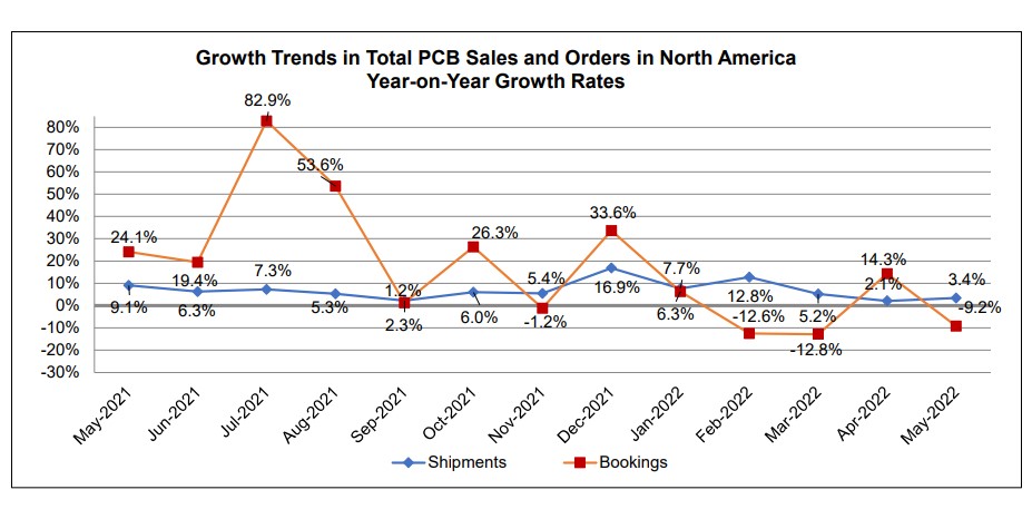
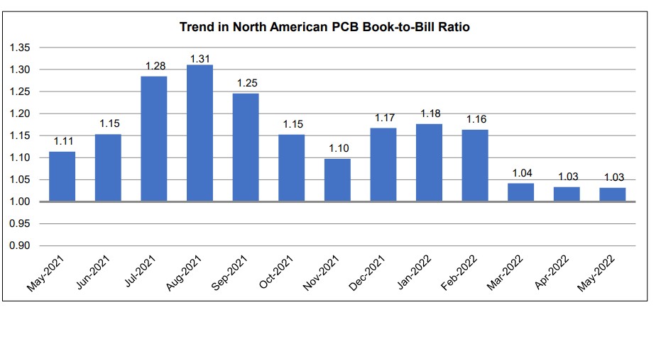
IPC announced today the May 2022 findings from its North American Printed Circuit Board (PCB) Statistical Program. The book-to-bill ratio stands at 1.03.

Total North American PCB shipments in May 2022 were up 3.4 percent compared to the same month last year. Compared to the preceding month, May shipments rose 1.1 percent.

PCB year-to-date bookings in May were down 9.2 percent compared to last year. Bookings in May fell 10.3 percent from the previous month.

“PCB demand remains strong and is showing some signs of normalization,” said Shawn DuBravac, IPC’s chief economist. “Order flow is slowing and shipments are picking up, bringing the book-to-bill into a more normal range.”

May 2022 PCB book to bill chart 1
May 2022 PCB book to bill chart 2

View charts in pdf format 

Detailed Data Available

Companies that participate in IPC’s North American PCB Statistical Program have access to detailed findings on rigid PCB and flexible circuit sales and orders, including separate rigid and flex book-to-bill ratios, growth trends by product types and company size tiers, demand for prototypes, sales growth to military and medical markets, and other timely data.

Interpreting the Data

The book-to-bill ratios are calculated by dividing the value of orders booked over the past three months by the value of sales billed during the same period from companies in IPC’s survey sample. A ratio of more than 1.00 suggests that current demand is ahead of supply, which is a positive indicator for sales growth over the next three to twelve months. A ratio of less than 1.00 indicates the reverse.

Year-on-year and year-to-date growth rates provide the most meaningful view of industry growth. Month-to-month comparisons should be made with caution as they reflect seasonal effects and short-term volatility. Because bookings tend to be more volatile than shipments, changes in the book-to-bill ratios from month to month might not be significant unless a trend of more than three consecutive months is apparent. It is also important to consider changes in both bookings and shipments to understand what is driving changes in the book-to-bill ratio.

IPC’s monthly PCB industry statistics are based on data provided by a representative sample of both rigid PCB and flexible circuit manufacturers selling in the USA and Canada. IPC publishes the PCB book-to-bill ratio by the end of each month.

PCB Manufacturability and Reliability Solutions for Fine Pitch PCB Server Boards

Member Download (pdf)

Industry demand for high-speed server product performance such as PCI express requires higher pin counts in order to support memory channels which in turn is driving pitch reduction in the printed circuit board(PCB).To provide better signal integrity for high-speed signals, ultra-low loss (ULL) PCB materials may need to be used, and back drilling is recommended to remove via stubs and minimize signal loss.  Back drilling is the process where by plated through holes(PTH)are drilled from the stub-side of the PCB with a larger drill diameter (i.e. back drill) to a specified depth in order to reduce the stub length. This improves signal integrity by minimizing interference or signal loss due to excess stub length. Current industry back drilling capabilities have supported greater than 1mm pitch with a minimum back drill-to-metal gap of greater than 0.15mm. For pitches < 1mm, the drill-to-metal gap will need to be reduced to less than 0.15 mm. In addition, primary drill(PD)diameters will need to scale down. These changes pose manufacturability challenges with primary drill registration and higher aspect ratios (i.e. PCB thickness/PD). Reduced spacing compounded with drill registration issues can result in exposed copper, slivers//clipped traces, and layer-to-layer misregistration. Industry PCB manufacturing capability and experience with these finer pitches is immature. Next-generation server platforms will push the limits of current PCB industry capabilities, creating a need to identify and provide solutions to enable future manufacturing technologies for server PCBs requiring < 1 mm (0.94 mm) pitch designs. This paper will assess PCB vendor drill registration capability and will also evaluate PCB reliability using electrochemical migration (i.e. conductive anodic filament or CAF) and via reliability (i.e. interconnect stress testing or IST) testing. PCB manufacturing capability will be characterized as a function of back drill-to-metal gap capability and provide potential solution paths to enable PCB suppliers to fabricate reliable 0.94 mm pitch server boards.

Author(s)
A.Caputo, W.C. Roth, B. Grossman, B. Aspnes, X. Ye, W. Acevedo, J. Landeros, and S.A. Aravamudhan
Resource Type
Technical Paper
Event
IPC APEX EXPO 2020